lunes, 7 de marzo de 2011

Valencia liderará la investigación europea en telecomunicaciones espaciales de alta potencia


La Agencia Espacial Europea (ESA) ha apostado por Valencia para la instalación de un laboratorio pionero y de referencia internacional en el ámbito de las telecomunicaciones espaciales. Se instalará en la Ciudad Politécnica de la Innovación, parque científico de la Universidad Politécnica de Valencia, y en el campus de Burjassot de la Universitat de València-Estudi General.

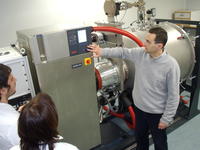
Investigadores del ITEAM de la UPV en el actual laboratorio experimental del Instituto para medidas de alta potencia en comunicaciones espaciales

Este laboratorio, que hasta ahora tenía su sede en Noordwijk (Holanda), se centrará en el estudio de los fenómenos de ruptura de radiofrecuencia en satélites y naves espaciales con señales de microondas de alta potencia así como en la validación de componentes de microondas para aplicaciones espaciales.

Otra de las actividades del laboratorio se enfocará en su apoyo a la industria europea ofreciendo sus recursos e instalaciones para calificar componentes europeos de alta potencia embarcados en satélites y así garantizar las comunicaciones con Tierra.

Val Space Consortium

A finales de 2009, la ESA firmó un preacuerdo con la Generalitat Valenciana –a través de la Conselleria d´Educació-, el Ayuntamiento de Valencia, la Universidad Politécnica de Valencia y la Universitat de València-Estudi General -que formarán el Val Space Consortium- en el que se sentaron las bases para la instalación en nuestra ciudad, durante los próximos meses, del mencionado laboratorio.

El laboratorio experimental se ubicará en las instalaciones de la Universidad Politécnica de Valencia, concretamente en la Ciudad Politécnica de la Innovación, y en la Facultad de Física de la Universitat de València-Estudi General.

Hasta la fecha, este laboratorio ha permanecido en el Centro Europeo de Investigación y Tecnología Espacial (ESTEC), que se encuentra en Noordwijk (Holanda), y que se encarga del diseño de la mayor parte de los satélites y del desarrollo tecnológico de la Agencia Espacial Europea.

Este laboratorio podría convertirse en un primer embrión para el desarrollo de un centro espacial en Valencia que albergaría otras disciplinas directamente relacionadas con la investigación espacial.

El laboratorio de la ESA se convertirá, además, en un foco de atracción de científicos europeos que acudirán a Valencia a formarse y a desarrollar sus investigaciones.


ELABORADO POR:

NERWIN ANTONIO MORA REINOSO

C.I: 17.557.095

CAF

Nuevos filtros de microondas mejorarán los sistemas de comunicación inalambricos


En su tesis Nuevas técnicas para la síntesis de dispositivos de microondas basadas en la Teoría de acoplo de modos, Israel Arnedo Gil, Ingeniero de Telecomunicación por la Universidad Pública de Navarra (UPNA), ha propuesto un nuevo método para diseñar filtros de microondas, unos dispositivos esenciales para controlar la cantidad de energía y el tiempo que ésta tarda en ir de un punto a otro del sistema.

El investigador, Israel Arnedo Gil

¿Qué tiene en común un horno microondas con los radares, las comunicaciones por satélite, la telefonía móvil o los sistemas inalámbricos? Todos ellos utilizan microondas y ondas milimétricas en su funcionamiento. En su tesis doctoral, "Nuevas técnicas para la síntesis de dispositivos de microondas basadas en la Teoría de acoplo de modos", Israel Arnedo Gil, Ingeniero de Telecomunicación por la UPNA, ha propuesto un nuevo método para diseñar filtros de microondas, unos dispositivos esenciales para controlar la cantidad de energía y el tiempo que ésta tarda en ir de un punto a otro del sistema. Su trabajo de investigación le ha permitido mejorar determinadas aplicaciones y obtener una patente internacional en explotación.

Los circuitos de microondas y ondas milimétricas se utilizan para generar, procesar y detectar señales electromagnéticas en un rango de frecuencia determinado —entre 1GHz y 300 GHz—. Sus aplicaciones son muy diversas: el radar (localización de personas, predicción del tiempo, control de tráfico aéreo o terrestre), la transmisión de información (telefonía, televisión, internet o datos) mediante enlaces terrestres de microondas (sistemas de repetidores) y espaciales (comunicaciones por satélite), los sistemas inalámbricos de comunicaciones, el calentamiento de alimentos y materiales y los receptores de alta sensibilidad para radioastronomía.

Todo este sinfín de aplicaciones necesita un elemento fundamental: el filtro de microondas. Su función, de modo muy simplificado, es dejar pasar unas ondas electromagnéticas y bloquear otras. El objetivo de la tesis doctoral de Israel Arnedo ha sido mejorar algunas aplicaciones y lo ha conseguido mejorando las herramientas con las que se diseñan esos filtros.

Estableciendo un paralelismo con la televisión podría decirse que si hasta ahora las técnicas de elaboración de filtros eran en blanco y negro, las técnicas de síntesis que ha desarrollado este ingeniero han traído el color. Entre las ventajas de su método frente a las técnicas clásicas, se encuentra que se obtienen soluciones para problemas que no los tenían; se obtienen soluciones más robustas de cara a la fabricación y producción en masa; y las soluciones obtenidas proporcionan mayor flexibilidad en los diseños.

Resultados exitosos para dispositivos clave

Las herramientas de síntesis diseñadas por Arnedo han sido utilizadas con éxito en tres grupos de aplicaciones: en la tecnología UWB (Ultra-Wideband), en el sector espacial y en el procesado de señales de radar.

La tecnología UWB se presenta como una evolución de las comunicaciones inalámbricas, al proporcionar mucha más flexibilidad de uso y servicios. Es también clave para implementar sistemas avanzados de seguridad (radio vigilancia) y de detección bajo tierra (personas sepultadas por terremotos, minas antipersona, etc).

Por eso, es de vital importancia que el diseño de emisores y receptores sea óptimo. En colaboración con el Institute National de la Recherche Scientifique INRS-EMT y la McGill University en Montreal, Canadá, Arnedo ha diseñado dos dispositivos que pueden ser claves para la generación (emisor) y recepción (receptor) de señales UWB.

En cuanto al sector espacial, el modo en que las estaciones en la tierra y los satélites se comunican debe ser óptimo para que la calidad de la señal recibida (por ejemplo, la televisión en nuestros hogares) sea alta. En este sentido, se ha propuesto una técnica robusta para el diseño de filtros, que ofrece mejoras frente a los utilizados en la actualidad, tanto desde el punto de vista de servicio como desde los costes.

Por último, para aplicaciones de radares con gran ancho de banda, las herramientas propuestas han permitido diseñar un dispositivo óptimo para el procesado analógico de señales a gran velocidad, lo que amplía las posibilidades de esta tecnología desde el punto de vista práctico

ELABORADO POR:

NERWIN ANTONIO MORA REINOSO

C.I: 17.557.095

CAF


Closing In On Quantum Computers


Researchers around the world are working on the development of quantum computers that will be vastly superior to present-day computers. Here, the strong coupling of quantum bits with light quanta plays a pivotal role. Professor Rudolf Gross, a physicist at the Technische Universitaet Muenchen (TUM), and his team of researchers have now realized an extremely strong interaction between light and matter that may represent a first step in this direction. The results of their research are presented in the current online issue of the journal Nature Physics.

Super conducting quantum circuit (c) TUM

Super conducting quantum circuit (c) TUM

The interaction between matter and light represents one of the most fundamental processes in physics. Whether a car that heats up like an oven in the summer due to the absorption of light quanta or solar cells that extract electricity from light or light-emitting diodes that convert electricity into light, we encounter the effects of these processes throughout our daily lives. Understanding the interactions between individual light particles – photons – and atoms is crucial for the development of a quantum computer.

Physicists from the Technische Universitaet Muenchen (TUM), the Walther-Meissner-Institute for Low Temperature Research of the Bavarian Academy of Sciences (WMI) and the Augsburg University have now, in collaboration with partners from Spain, realized an ultrastrong interaction between microwave photons and the atoms of a nano-structured circuit. The realized interaction is ten times stronger than levels previously achieved for such systems.

The simplest system for investigating the interactions between light and matter is a so-called cavity resonator with exactly one light particle and one atom captured inside (cavity quantum electrodynamics, cavity QED). Yet since the interaction is very weak, these experiments are very elaborate. A much stronger interaction can be obtained with nano-structured circuits in which metals like aluminum become superconducting at temperatures just above absolute zero (circuit QED). Properly configured, the billions of atoms in the merely nanometer thick conductors behave like a single artificial atom and obey the laws of quantum mechanics. In the simplest case, one obtains a system with two energy states, a so-called quantum bit or qubit.

Coupling these kinds of systems with microwave resonators has opened a rapidly growing new research domain in which the TUM Physics, the WMI and the cluster of excellence Nanosystems Initiative Munich (NIM) are leading the field. In contrast to cavity QED systems, the researchers can custom tailor the circuitry in many areas.

To facilitate the measurements, Professor Gross and his team captured the photon in a special box, a resonator. This consists of a superconducting niobium conducting path that is configured with strongly reflective "mirrors" for microwaves at both ends. In this resonator, the artificial atom made of an aluminum circuit is positioned so that it can optimally interact with the photon. The researchers achieved the ultrastrong interactions by adding another superconducting component into their circuit, a so-called Josephson junction.

The measured interaction strength was up to twelve percent of the resonator frequency. This makes it ten times stronger than the effects previously measureable in circuit QED systems and thousands of times stronger than in a true cavity resonator. However, along with their success the researchers also created a new problem: Up to now, the Jaynes-Cummings theory developed in 1963 was able to describe all observed effects very well. Yet, it does not seem to apply to the domain of ultrastrong interactions. "The spectra look like those of a completely new kind of object," says Professor Gross. "The coupling is so strong that the atom-photon pairs must be viewed as a new unit, a kind of molecule comprising one atom and one photon.

Experimental and theoretical physicists will need some time to examine this more closely. However, the new experimental inroads into this domain are already providing researchers with a whole array of new experimental options. The targeted manipulation of such atom-photon pairs could hold the key to quanta-based information processing, the so-called quantum computers that would be vastly superior to today's computers.

The research was funded by the Deutsche Forschungsgemeinschaft (DFG) (Cluster of Excellence Nanosystems Initiative Munich and SFB 631), the European Community (EuroSQIP, SOLID), as well as the Spanish Ministry for Science and Innovation.


ELABORADO POR:

NERWIN ANTONIO MORA REINOSO

C.I: 17.557.095

CAF

ANTENAS


¿Que son las antenas y cuales son sus caracteristicas?

La definición formal de una antena es un dispositivo que sirve para transmitir y recibir ondas de radio. Convierte la onda guiada por la línea de transmisión (el cable o guía de onda) en ondas electromagnéticas que se pueden transmitir por el espacio libre.
En realidad una antena es un trozo de material conductor al cual se le aplica una señal y esta es radiada por el espacio libre.


Una antena transmisora es un dispositivo que transforma las ondas que se propagan en líneas de transmisión o guías de onda en ondas radiadas.


Una antena receptora es un dispositivo capaz de captar ondas electromagnéticas y transformarlas en ondas guiadas.


Las características de las antenas dependen de la relación entre las dimensiones y la longitud de onda de la señal de radiofrecuencia transmitida o recibida. Si las dimensiones de la antena son mucho más pequeñas que la longitud de onda, las antenas se denominan elementales. Las antenas resonantes tienen dimensiones del orden de media longitud de onda. Las antenas cuya dimensión es de varias longitudes de onda tienen una gran directividad.


Tipos de antenas:


Existen varios tipos de antena acontnuacion mostrare algunas imagenes:


ELABORADO POR:

NERWIN ANTONIO MORA REINOSO

C.I: 17.557.095

CAF


(microondas)Descubierta una rara fuente estelar de agua


Se han descubierto tres nuevos másers de agua en la Vía Láctea, incluyendo el que podría ser uno de los más rápidos jamás encontrados – alcanzando velocidades de hasta 350 km por segundo – y uno raro del tipo "fuente de agua".

Las fuentes de agua son una clase especial de 'máser' – grandes lásers de microondas provocados por estrellas moribundas de gran masa o por regiones de formación estelar muy masivas. La fuente masiva expulsa material incluyendo nubes de agua que pueden viajar a un par de cientos de kilómetros por segundo.

Descubierta una rara fuente estelar de agua image"A esta velocidad [350 km/s] sería posible viajar desde Sydney a Londres en sólo un minuto", dice Glen Rees de programa de vacaciones de verano de CSIRO, que encontró los tres másers usando datos recopilados por el Estudio del Plano Galáctico Austral de H2O (HOPS).

Cuando las moléculas de agua absorben energía

El término máser se originó como acrónimo de Microwave Amplification by Stimulated Emission of Radiation (Amplificación de Microondas por la Emisión de Radiación Estimulada). Los másers funcionan de la misma forma que los lásers, excepto que emiten microondas en lugar de luz visible.

Las moléculas de agua en las Regiones de Formación Estelar de Gran Masa (HMSR) y alrededor de estrellas moribundas absorben energía de sus alrededores y la re-emiten como radiación en el rango de frecuencias de las microondas.

Usando el Conjunto Australiano Compacto de Telescopios (ATCA) cerca de Narrabri en Nueva Gales del Sur, Rees investigó las características de tres máser únicos de agua situados en la Vía Láctea buscando una frecuencia de radiación concreta en la región de microondas que es característica de los másers de agua. "Los másers de agua emiten en los 22 Giga-Hertz por lo que llevamos a cabo nuestras observaciones en esta frecuencia", comenta Rees.

Sólo se han encontrado 12 fuentes de agua

Uno de los másers de agua que descubrió Rees se encontró alrededor de una estrella de Rama post-Asintótica Gigante (AGB) – una estrella cerca del final de su vida – y que cae bajo la clasificación de 'fuente de agua' para los másers de agua.

Las 'fuentes de agua' tienen lugar cuando una estrella moribunda expulsa chorros de molécula de agua cuando realiza la transición a la siguiente etapa de su vida.  Sólo se han detectado hasta el momento 12 fuentes de agua.

Estas 'fuentes de agua' estelares pueden ayudan a los científicos a descubrir cómo las estrellas esféricas AGB evolucionan hacia nebulosas planetarias – una brillante y colorida cobertura de gas y polvo alrededor de una estrella en las últimas etapas de su vida, que muestra una variedad de formas y tamaños.

"Exactamente cómo se forman las estrellas de gran masa es algo que no se comprende aún por completo, y los másers de agua pueden dar una valiosa visión en el proceso implicado", dice Rees.

Un máser 'alocadamente rápido'

Otro de los másers de agua que Rees está estudiando se ha confirmado como el máser de agua más rápido encontrado en un HMSR con velocidades de hasta 200 km por segundo. La velocidad media de un máser de agua normalmente ronda los 27 a 30 km por segundo.

El tercer máser de agua, que tiene una velocidad de 350 km por segundo y Rees está tratando de determinar si está en un HMSR o alrededor de una estrella post-AGB, es 'alocadamente rápido'.

Si el máser de agua está en un HMSR será el más rápido conocido en este grupo, batiendo al otro máser de agua.

Los ejemplos más extremos conocidos

El físico Simon Ellingsen de la Universidad de Tasmania, que no estuvo implicado en el estudio, comenta: "Estas tres fuentes representan los ejemplos más extremos conocidos hasta la fecha tanto en estrellas post-AGB como el regiones de formación estelar de gran masa".

"Los ejemplos más extremos son particularmente importantes ya que proporcionan las mejores pruebas para las teorías sobre cómo se producen estos flujos", señala Ellingsen.

Otros científicos están investigando otros tipos de másers, incluyendo metanol, hidroxilo y formaldehído, para ayudar a descubrir más sobre cómo las estrellas y galaxias cambian con el tiempo.


ELABORADO POR:

NERWIN ANTONIO MORA REINOSO

C.I: 17.557.095

CAF

Three-dimensional waveguide junctions inside glass


In photonic devices and networks, optical waveguides routinely need to be coupled, split, and switched; several methods are in use to fabricate those junctions. A promising technique for making three-dimensional junctions in transparent materials, such as silica glass, is to write them with femtosecond lasers. Under optimal laser-writing conditions, a focused spot photoexcites the glass through nonlinear absorption and locally changes the refractive index. Slowly moving the material stretches the spot into a line of altered index that acts as a waveguide. For creating junctions, however, it has proven difficult to precisely position the material for each branch. Now, researchers at Japan's Kyoto University have sidestepped that issue by introducing parallel laser writing of multiple branches in three dimensions. The key is computer-generated holograms. With a CGH and a single laser, multiple beam spots can be focused at precise locations in the glass. As the material is moved, CGHs are sequentially swapped in and out to change the spots' locations. Using 256 CGHs, the researchers fabricated a 20-mm-long continuous waveguide that split and spread into four branches about 85 µm apart. A schematic is shown on the left, and the output from a single incident 635-nm laser beam is shown on the right. Optimization of the method is under way. (M. Sakakura et al., Opt. Express 18, 12136, 2010.)—Stephen G. Benka


ELABORADO POR:

NERWIN ANTONIO MORA REINOSO

C.I: 17.557.095

CAF

New research advances with surface plasmon polariton waveguides


(Nanowerk News) On February 23, "Plasmonic Coupling of Bow Tie Antennas with Ag Nanowire" written by Fang Zheyu and his colleagues from the School of Physics at Peking University (PKU) was published in the journal Nano Letter and was highly regarded by referees. This work is done on the basis of research on surface plasmon polariton (SPP) by near-field optics technology and is the second paper published in Nano Letters in the past two months by Fang Zheyu, a Ph.D. candidate, under the guide of Professor Zhu Xing.
One of the key problems of nano-scale optical devices is how to guide and propagate incident light effectively. SPP waveguide has a long propagating distance and can transmit in metal-dielectric interface. How to enhance the coupling and transmission of SPP has attracted researchers' attention at present. Recently, Prof. Zhu Xing et al. has found a new way to improve coupling between light and SPP and realize an enhanced SPP emission with a factor of 45 by using impedance matching theory and high-precision micro-nano processing. They put bow tie nano-optical antennas at both ends of Ag nanowire with mathematical precision to realize an enhanced SPP coupling of Ag bow tie antennas. They also realize effective coupling of SPP at incident side of Ag nanowire by using impedance matching theory and changing the length of Ag nanowire, the arm length of bow tie antennas, and the incident angle of optical excitation, providing a new method in optical coupling and transmission of nano-scale optical devices.
This research, supported by National Special Science Research Program of the Ministry of Science and Technology, National Natural Science Foundation, and State Key Laboratory for Mesoscopic Physics of PKU, is jointly completed by PKU, National Center for Nanoscience and Technology, China (NCNST), and Tübingen University.

ELABORADO POR:

NERWIN ANTONIO MORA REINOSO

C.I: 17.557.095

CAF


The future of Fiber Optic Communication


All-Optical Network

All-optical network has been a top topic in fiber optic communication industry for over a decade now. Its ultimate goal is to process all signals in the optical domain without any conversion and controlling to electrical domain at all.

At least for now, most signal routing, processing and switching happens in the electrical domain. Optical signals have to be converted to electrical signal first, and then the electrical signals are processed, routed and switched to their final destination.

After the processing, routing and switching, the electrical signals are then converted back to optical signals which are then transmitted over long distances. This process is called the O-E-O process.

But this O-E-O process severely limits the speed of the network. Why? Since optical signals can process data much faster then today's electronics. The O-E-O process has been a bottleneck preventing us from achieving even higher data rates.

This bottleneck creates a tremendous interest in all-optical networks where no electronics are needed for signal processing, routing and switching. Another big benefit of all-optical network is that since all signal processing, routing and switching happens in optical domain, there is no need to replace the electronics when data rates increase. For example, current fiber optic transmitters and receivers can handle only one single data rate, thus, they must be replaced when the data rate increases. This won't be necessary in a all-optical network.

However, many obstacles still lie in our way to make all-optical network a reality. Some functions such as reading headers on the optical signals, switching the optical signal on the fly based on the header content and real-time wavelength switching are just a few of the serious challenges that need to be solved before we can have a true all-optical network.

Multi-Terabit Networks

DWDM opens the door to multi-terabit transmission. The interest in developing multi-terabit networks is driven by the increasing availability of more bandwidth in fiber optic networks.

One terabit network was achieved by using 10Gb/s data rate combined with 100 DWDM channels.

Four terabit network can be achieved by combing 40Gb/s data rate with 100 DWDM channels too. Researchers move their target to even higher bandwidth with 100Gb/s systems. (Which is not a reality yet, at least for now)

But this kind of speed is very expensive to make and can only be justified on long-haul systems. But with the cost reduction on fiber optic components, devices and systems, more bandwidth is not far from us.

There are some other major trends in the fiber optic industry too. The most important ones include expansion into mass markets (FTTH, FTTB, FTTC, etc), miniaturization, new technology development, cost reductions and even more.


ELABORADO POR:

NERWIN ANTONIO MORA REINOSO

C.I: 17.557.095

CAF

What is a VSWR?


VSWR (Voltage Standing Wave Ratio) is a metric commonly used with antenna systems used for ham or shortwave radio communication. VSWR is normally defined as a ratio with a 1:1 VSWR indicating that there is an exact or perfect match between all antenna system elements. The VSWR can also be expressed through comparing Vmax against Vmin in a ratio.

VSWR

Why Does VSWR Exist?

In order to obtain the maximum power from a load requires that the load and generator impedance match. If there is any mismatch or difference, then maximum power transfer does not occur. This same concept also applies to antennas and transmitters. Since the antenna is normally located at distance from the transmitter, the feed-line has not have no loss and match both the antenna input impedance and transmitter output impedance to have a VSWR of 1:1. The resulting voltage and current would then have to be constant over the length of the feed-line. If there is any deviation from this circumstance, then there will be a standing wave of voltage and current created and the VSWR will exceed the 1:1 ratio.

How is VSWR Measured?

VSWR and its effects can be measured in several ways to include return loss, reflected power, reflection coefficient, and transmitted power loss. These all measure the proportion of power that is reflected back to the transmitter by a mismatched antenna just in different ways. The reflection coefficient is a measure of the mismatch at the antenna by the feed-linee and is expressed by the following formula, P =(Z1-Zo)/(Z1+Zo). Z1 refers to the antenna impedance and Z0 refers to the feed-line impedance with all variables being complex numbers. When Z1 = Zo there is no reflected signal in the antenna system. This condition is rarely seen, however, and is used more in antenna theory than in practical antenna applications.

Where are VSWR Measurements Made?

Along an antennas feed-line, the voltages will have a voltage minimum and maximum based on the relative phase difference of the traveling waves along the line. The minimum and maximum points normally occur ¼ wavelength apart from each other. Since the adoption of coaxial cable in antenna systems, VSWR measurements are normally made on the transmitter end of the feed-line.


ELABORADO POR:

NERWIN ANTONIO MORA REINOSO

C.I: 17.557.095

CAF

Scheme of Standing Wave Ratio (SWR)


Scheme of Standing Wave Ratio (SWR)

In telecommunications for example Communication and WiFi HT 2.4 MHz or 5.8 MHz, standing wave ratio (SWR) is the partial wave amplitude ratio stood at antinode (maximum) for amplitude in an adjacent node (minimum), in electrical transmission lines.
SWR is usually defined as the ratio of voltage is called the VSWR, for voltage standing wave ratio. For example, the value of standing wave VSWR 1.2:1 shows the maximum amplitude is 1.2 times larger than the minimum value of standing waves. It is also possible to define the SWR in terms of currents, yield ISWR, which has the same numerical value. The power standing wave ratio (PSWR) VSWR is defined as the square.
Practical implications of the SWR.
The most common one to measure and check the SWR is when installing and tuning the transmission antenna. When the transmitter is connected to the antenna feed line, the impedance of the antenna and feed lines must be identical to the maximum energy transfer from the feed line to the antenna becomes possible. Impedance of the antenna varies based on many factors, including: the natural resonance frequency of the antenna on that is being sent, the antenna height above ground, and the size of conductor used to make antenna.
When the antenna and feedline has no impedance matching, several electrical energy can not be transferred from the feedline to the antenna. Energy is not transferred to the antenna is reflected back to receiver. It is the interaction of these waves are reflected by the forward wave which causes the standing wave pattern. Reflected power has three major implications on radio transmitters: Radio Frequency (RF) energy loss increases, the distortion in the transmitter because the reflected power from the transmitter load and damage can occur

SWR-Matching Impedance

Matching the impedance of the antenna to the impedance of the feed line is usually done by using an antenna tuner. tuner can be plugged in between the transmitter and the feed line, or between the feed lines and antennas. Both methods of installation will allow the transmitter to operate at a low SWR, but if the tuner is mounted on the transmitter, feed line between the tuner and antenna will still operate with a high SWR, causing additional RF energy to be lost through the feedline.
Many amateur radio operators to consider the problem serious impedance mismatch. However, this does not happen. Assuming the discrepancy is within the limits of operation of these transmitters, radio operators only need to worry about the loss of power on the transmission line. Power loss will increase with increasing SWR, but this increase is often less than might consider many amateur radio. For example, a dipole antenna tuned to operate at 3.75MHz center of the 80-meter-band radio amateurs will show SWR around 6:01 on the outskirts of the band. However, if the antenna was given with 250 feet of coax RG-8A, losses due to standing waves of only 2.2dB. Feed line loss typically increases with frequency, so antenna VHF and above must match closely with the feedline. 6:01 mismatch equal to 250 feet of RG-8A coax will cause harm to 10.8dB 146MHz.


ELABORADO POR:

NERWIN ANTONIO MORA REINOSO

C.I: 17.557.095

CAF

Standing Waves


Whenever there is a mismatch of impedance between transmission line and load, reflections will occur. If the incident signal is a continuous AC waveform, these reflections will mix with more of the oncoming incident waveform to produce stationary waveforms called standing waves. The following illustration shows how a triangle-shaped incident waveform turns into a mirror image reflection upon reaching the line's unterminated end. The transmission line in this illustrative sequence is shown as a single, thick line rather than a pair of wires, for simplicity's sake. The incident wave is shown traveling from left to right, while the reflected wave travels from right to left: (Figure 18.1) If we add the two waveforms together, we find that a third, stationary waveform is created along the line's length: (Figure 18.2)

 Incident wave reflects off end of unterminated transmission line.Figure 18.1: Incident wave reflects off end of unterminated transmission line.

This voltage standing wave ratio, "standing" wave, in fact, represents the only voltage along the line, being the representative sum of incident and reflected voltage waves. It oscillates in instantaneous magnitude, but does not propagate down the cable's length like the incident or reflected waveforms causing it. Note the dots along the line length marking the "zero" points of the standing wave (where the incident and reflected waves cancel each other), and how those points never change position: (Figure 18.3)

 The sum of the incident and reflected waves is a stationary wave.

Figure 18.2: The sum of the incident and reflected waves is a stationary wave.

 The standing wave does not propagate along the transmission line.Figure 18.3: The standing wave does not propagate along the transmission line.

One way of expressing the severity of standing waves is as a ratio of maximum amplitude (antinode) to minimum amplitude (node), for voltage or for current. When a line is terminated by an open or a short, this standing wave ratio, or SWR is valued at infinity, since the minimum amplitude will be zero, and any finite value divided by zero results in an infinite (actually, "undefined") quotient. In this example, with a 75 line terminated by a 100 impedance, the SWR will be finite: 1.333, calculated by taking the maximum line voltage at either 250 kHz or 750 kHz (0.5714 volts) and dividing by the minimum line voltage (0.4286 volts). Standing wave ratio may also be calculated by taking the line's terminating impedance and the line's characteristic impedance, and dividing the larger of the two values by the smaller. In this example, the terminating impedance of 100 divided by the characteristic impedance of 75 yields a quotient of exactly 1.333, matching the previous calculation very closely. Standing wave ratio are as given

A perfectly terminated transmission line will have an SWR of 1, since voltage at any location along the line's length will be the same, and likewise for current. Again, this is usually considered ideal, not only because reflected waves constitute energy not delivered to the load, but because the high values of voltage and current created by the antinodes of standing waves may over-stress the transmission line's insulation (high voltage) and conductors (high current), respectively.


ELABORADO POR:

NERWIN ANTONIO MORA REINOSO

C.I: 17.557.095

CAF